MYSHOP
최근 본 상품


| 상품명 | MC33926 Motor Driver Carrier |
|---|---|
| 판매가 | 26,636원 |
| 적립금 | 200원 (1%) |
| 상품코드 | P000EBWD |
| 수량 |   |
| 세액 | 2,664원 |
| 공급사 | Pololu |
| SNS 상품홍보 |
|---|

 |
(최소주문수량 1개 이상 / 최대주문수량 0개 이하)
사이즈 가이드 수량을 선택해주세요.
위 옵션선택 박스를 선택하시면 아래에 상품이 추가됩니다.
| 상품명 | 상품수 | 가격 |
|---|---|---|
| MC33926 Motor Driver Carrier |   |
( |
총 상품금액(수량) : 0 (0개)

|
||
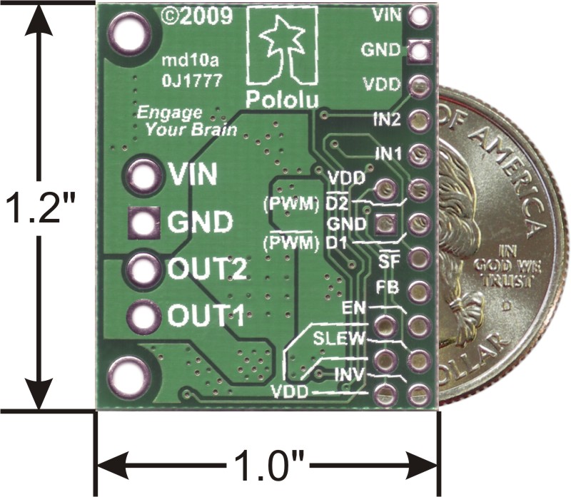 |
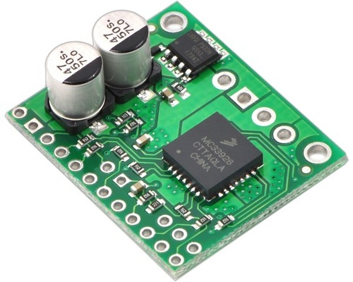
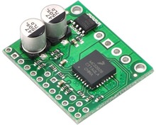
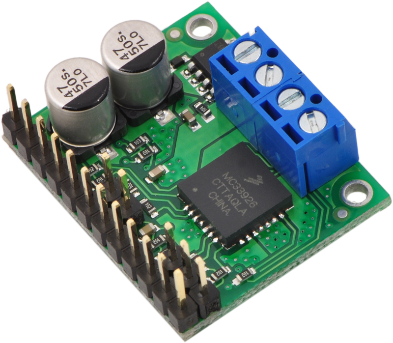
The MC33926 motor driver carrier can supply up to almost 3 A continuous current to a single brushed DC motor at 5 – 28 V, and it can tolerate peak currents up to 5 A for a few seconds, making this a great general-purpose motor driver for medium-sized DC motors. The MC33926 supports ultrasonic (up to 20 kHz) pulse width modulation (PWM) of the motor output voltage, which eliminates the audible switching sounds caused by PWM speed control, and a current feedback circuit outputs an analog voltage on the FB pin that is proportional to the output current. Since this board is a carrier for the Freescale Semiconductor MC33926 H-bridge, we recommend careful reading of theMC33926 datasheet (1MB pdf).
If you have two motors to control, please consider the Dual MC33926 motor driver carrier.
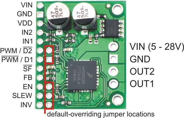 |
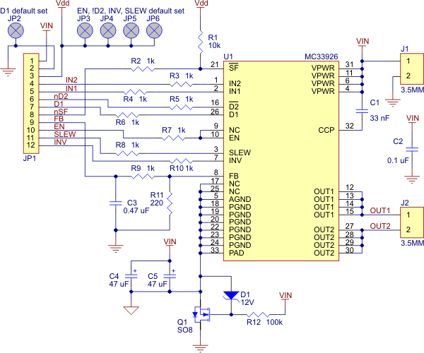
The default states of many of the MC33926 logic input pins requires that many external connections be made to use this motor driver. To reduce the number of necessary external connections, the board has five default-overriding jumpers. All of the default-overriding jumpers are tied to VDD, except the D1 jumper, which is tied to GND. All VDD jumper pads are circles; the ground jumper pad is square.
| PIN | Default State | Description |
|---|---|---|
| VIN | HIGH | This is the main 5 – 28 V motor power supply connection, which should typically be made to the larger VIN pad. Operation from 5 – 8 V reduces maximum current output; the device is also protected for transients up to 40 V. The smaller VIN pad can be used to distribute the VIN node to the rest of the application circuit; for lower-current applications, the pin can also be used to power the motor driver and motor. |
| GND | LOW | Ground connection for logic and motor power supplies. |
| OUT2 | HIGH | The motor output pin controlled by IN2. |
| OUT1 | HIGH | The motor output pin controlled by IN1. |
| VDD | HIGH | 3-5 V logic supply connection. This pin is used only for theSF pull-up and default-overriding jumpers; in the rare case where none of those features is used, VDD can be left disconnected. |
| IN2 | HIGH | The logic input control of OUT2. PWM can be applied to this pin (typically done with both disable lines inactive). |
| IN1 | HIGH | The logic input control of OUT1. PWM can be applied to this pin (typically done with both disable lines inactive). |
| PWM / D2 | LOW | Inverted disable input: when D2 is low, OUT1 and OUT2 are set to high impedance. A D2 PWM duty cycle of 70% gives a motor duty cycle of 70%. Typically, only one of the two disable pins is used, but the default is for both disable pins to be active. |
| PWM / D1 | HIGH | Disable input: when D1 is high, OUT1 and OUT2 are set to high impedance. A D1 PWM duty cycle of 70% gives a motor duty cycle of 30%. Typically, only one of the two disable pins is used, but the default is for both disable pins to be active. |
| SF | HIGH | Status flag output: an over-current (short circuit) or over-temperature event will cause SF to be latched LOW. If either of the disable pins (D1 or D2) are disabling the outputs, SFwill also be LOW. Otherwise, this pin is weakly pulled high. This allows the SF pins of multiple units to connected to a single input. |
| FB | LOW | The FB output provides analog current-sense feedback of approximately 525 mV per amp. |
| EN | LOW | Enable input: when EN is LOW, the chip is in a low-current sleep mode. |
| SLEW | LOW | Output slew rate selection input. A logical LOW results in a slow output rise time (1.5 μs – 6 μs). A logical HIGH selects a fast output rise time (0.2 μs – 1.45 μs). This pin should be set HIGH for high-frequency (over 10 kHz) PWM. |
| INV | LOW | A logical high value inverts the meaning of IN1 and IN2. This allows INV to function as a direction line if IN1 and IN2 are set to different values. |
In a typical application, five I/O lines are used to connect the motor driver to a microcontroller: the two input lines, IN1 and IN2, for direction control, one of the disable lines, D1 or D2, for PWM speed control, the status flag, SF, for monitoring motor driver errors, and the current sense output, FB, for monitoring motor current draw (connected to an analog-to-digital converter input). The control lines can be reduced to two pins if PWM signals are applied directly to the two input pins with both disable pins held inactive. A two-pin interface can also be achieved using one of the disable lines for PWM speed control and the INV input for direction control with IN1 and IN2 held at different values (i.e. one set HIGH and the other set LOW). In each of these cases, the other unused lines must be set to enable proper operation. For example, if D2 is used for the PWM input (as is typically the case), D1 must be held low to prevent it from disabling the motor driver. The circuit board provides convenient jumper points for overriding the motor driver defaults without having to connect extra wires to the module.
The current sense and status flag connections are optional, though monitoring of the status flag can allow detection of latched fault conditions. The status flag is an open-drain output, so multiple units can have their status flag pins wired together for applications where I/O pins are scarce and determining which motor driver is experiencing a fault condition is not necessary.
Note that the default state of the enable pin, EN, is LOW, which holds the chip in a low-current sleep mode. You will need to hold this pin high (either with an external connection or via the default-overriding jumper next to the pin) to allow the chip to run.
The MC33926 has under-voltage, over-current, and over-temperature protection. Some protection events are indicated by the status flag pin (SF), which is an active-low pin allowing the SF pin from multiple boards to connected to a single input. If the chip detects an over-current or over-termperature event, the SF is latched LOW and OUT1 and OUT2 are set to high-impedance. To unlatch the status flag pin toggle the D1, D2 , EN or VIN lines. The carrier board has a reverse-protection MOSFET for added protection to the motor driver chip.
The MC33926 motor driver used on the carrier board has a maximum current rating of 5 A continuous. However, the chip by itself will overheat at lower currents. For example, in our tests at room temperature with no forced air flow, the chip was able to deliver 5 A for 5 s and 4 A for 18 s before the chip’s thermal protection started reducing the current. A continuous current of 3 A was right at the over-temperature threshold; in some tests the thermal protection kicked in after a minute, and in other tests the chip delivered 3 A for over five minutes without triggering thermal protection. The actual current you can deliver will depend on how well you can keep the motor driver cool. The carrier’s printed circuit board is designed to draw heat out of the motor driver chip, but performance can be improved by adding a heat sink. Our tests were conducted at 100% duty cycle; PWMing the motor will introduce additional heating proportional to the frequency.
This product can get hot enough to burn you long before the chip overheats. Take care when handling this product and other components connected to it.
Unlike other H-Bridges, the 33926 has a feature that allows it to gracefully reduce current as the current exceeds 5 A or as the chip temperature approaches its limit. This means that if you push the chip close to its limit, you will see less power to the motor, but it might allow you to avoid a complete shutdown.
|
|
A 20-pin straight breakaway male header is included with the MC33926 carrier board, which can be used to connect the PCB to perfboards or breadboards. The board also includes two 2-pin 3.5mm terminal blocks for making simple motor connections.
 |
* 세금계산서 발행방법은 게시판 공지사항 참조.
* 기술문의는 이메일(master@toolparts.co.kr)로 문의.
전자부품 특성상 제품에 이상이 있거나, 상품정보와 상이한 경우 외 에 단순 고객변심으로는
교환 반품이 불가능 합니다 구매전 이점 유의해 주세요!!!
고액결제의 경우 안전을 위해 카드사에서 확인전화를 드릴 수도 있습니다. 확인과정에서 도난 카드의 사용이나 타인 명의의 주문등 정상적인 주문이 아니라고 판단될 경우 임의로 주문을 보류 또는 취소할 수 있습니다.
무통장 입금은 상품 구매 대금은 PC뱅킹, 인터넷뱅킹, 텔레뱅킹 혹은 가까운 은행에서 직접 입금하시면 됩니다.
주문시 입력한 입금자명과 실제입금자의 성명이 반드시 일치하여야 하며, 7일 이내로 입금을 하셔야 하며 입금되지 않은 주문은 자동취소 됩니다.
교환 및 반품이 가능한 경우
- 상품을 공급 받으신 날로부터 7일이내 단, 가전제품의
경우 포장을 개봉하였거나 포장이 훼손되어 상품가치가 상실된 경우에는 교환/반품이 불가능합니다.
- 공급받으신 상품 및 용역의 내용이 표시.광고 내용과
다르거나 다르게 이행된 경우에는 공급받은 날로부터 3월이내, 그사실을 알게 된 날로부터 30일이내
교환 및 반품이 불가능한 경우
- 고객님의 책임 있는 사유로 상품등이 멸실 또는 훼손된 경우. 단, 상품의 내용을 확인하기 위하여
포장 등을 훼손한 경우는 제외
- 포장을 개봉하였거나 포장이 훼손되어 상품가치가 상실된 경우
(예 : 가전제품, 식품, 음반 등, 단 액정화면이 부착된 노트북, LCD모니터, 디지털 카메라 등의 불량화소에
따른 반품/교환은 제조사 기준에 따릅니다.)
- 고객님의 사용 또는 일부 소비에 의하여 상품의 가치가 현저히 감소한 경우 단, 화장품등의 경우 시용제품을
제공한 경우에 한 합니다.
- 시간의 경과에 의하여 재판매가 곤란할 정도로 상품등의 가치가 현저히 감소한 경우
- 복제가 가능한 상품등의 포장을 훼손한 경우
(자세한 내용은 고객만족센터 1:1 E-MAIL상담을 이용해 주시기 바랍니다.)
※ 고객님의 마음이 바뀌어 교환, 반품을 하실 경우 상품반송 비용은 고객님께서 부담하셔야 합니다.
(색상 교환, 사이즈 교환 등 포함)
상품의 사용후기를 적어주세요.
게시물이 없습니다


상품에 대해 궁금한 점을 해결해 드립니다.
게시물이 없습니다